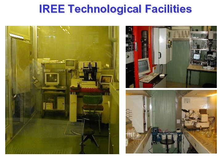
 Research Activities
|
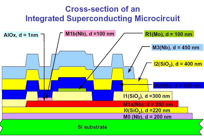
2. Technology for fabrication of superconducting integrated
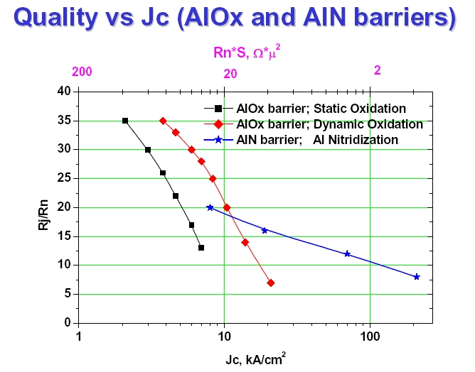
circuits based on S uperconductor - Insulator - Superconductor (SIS) tunnel junctions are basic elements of most superconducting electronic circuits. Therefore, a reliable and reproducible technology of SIS tunnel junction fabrication is a necessary condition to investigate superconducting high frequency devices. The objective is to optimize the fabrication of high quality Nb-AlOx-Nb micron-sized tunnel junctions and integrated circuits. A reliable process for fabrication of high quality Nb-AlOx-Nb tunnel junctions of micrometer size with current density up to 20 kA/cm2 has been developed. On the basis of this process a technology for fabrication of the superconducting microcircuits (up to 12 different layers) has been developed. A number of integrated circuits to measure the emission from a superconducting local oscillator (FFO) as well as microcircuits of an integrated receivers and spectrometer have been fabricated.To achieve the ultimate performance of integrated submm receivers with operational frequency up to 1 THz, tunnel junctions with an ultra transparent AlN tunnel barrier (current density up to 200 kA/cm2) have been developed. Utilization of the AlNx tunnel barrier, produced by Al nitridation in a nitrogen glow discharge, enables to produce high quality SIS junctions with low RnS values (a product of junction resistance and area, RnS as low as 1 Ω μm2 has been measured). To take advantage of the high transparency of an AlN tunnel barrier, it is important to fabricate sub-micrometer sized junctions. To achieve this task we have put in place reliable Chemical-Mechanical Polishing (CMP) processing using a Tech. Prep 8 polishing machine from Allied High Tech Products Inc. Electron Beam Lithography (EBL) has been incorporated to reduce junction area down to 0.03 μm2. Such small junctions are very important since the required LO power is proportional to the area of the SIS mixer junctions. Muli-element Josephson structures based on high-quality Nb-AlOx-Nb tunnel junctions of micron size with a number of the elements up to 1000 have fabricated and tested; an optimization of the technology has been performed in order to increase the integration level and yield.
|
|
Home | Staff | Activities | Publications | Collaboration | VirtualVisit | Links | |