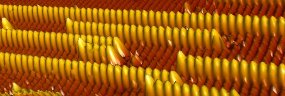
More than 300 surface reconstructions are already known for pure Si surface and Si surface with adsorbate. Study of their properties by the methods of surface physics reveal numerous interesting phenomena including various phase transitions accompanied by changes of Fermi-surface topology, development of the charge-density wave, etc. Much better understanding of these phenomena can by obtained from studying of electron transport, local energy structure and other electronic properties of these reconstructed surfaces.
Being negligible in 3-D case, electron–electron correlation effects play the
dominant role in one dimension. As a result, the physical properties of a one-dimensional
metal are expected to be dramatically different from those of usual metals with a Fermi
liquid of electrons. Earlier studies of conduction in nanowires made of semiconductors and quasi-1D conductors reveal very interesting properties of such systems. Atomic-scale wires may have even more exciting features that can be studied in much finer details.
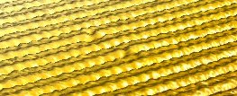
The charge-density wave (CDW) develops in materials with a chain-like crystal structure at temperatures below the Peierls transition temperature. The CDW can be considered as an electronic crystal existing inside a real crystal. Ability of the CDW to carry the electric charge and the periodic nature of the CDW leads to numerous collective phenomena, such as non-linear I-V curves, generation of narrow-band noise, appearance of Shapiro steps under RF irradiation etc. Whether or not similar phenomena can be observed in surface CDW is an interesting question.
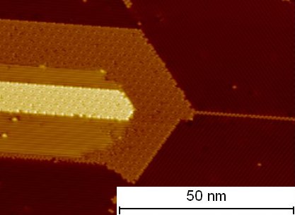
Atomic-scale quantum wires, quantum contacts, multibarrier systems and superstructures, quantum interferometers and many other systems can be formed by using self-organization or atomic manipulation on atomically-clean surfaces of metals, semiconductors or dielectrics. Scanning atomic-force/tunneling microscopy and scanning tunneling spectroscopy are ultimate tools to study electronic properties of such systems with atomic resolution.


_small.jpg)