PLASMA PROCESSING REACTOR ON A BASE OF BEAM PLASMA DISCHARGE
Scientific supervisor: Evgeniy G. SHUSTIN, Dr. Sc.,
head of research group of Kotel'nikov IRE RAS (Fryazino branch),
Tel. (7-49656)52569 E-mail:
shustin@ms.ire.rssi.ru
In plasma processing reactors used for
deposition of thin films, etching and surface modification of materials for nano-
and microelectronics, control of characteristics of the ions acting upon the
processed material is highly important for the optimization of the quality of
processing. In ion etching, an ion energy distribution function (FRIE) and an
angular dispersion of ions reaching the surface of the material have critical influence
on the speed and level of anisotropy of etching. Control of the spatial
distribution of the bombarding particles is important for the deposition of
films with a very homogeneous structure.
At IRE RAS the effect of ion beam emission
from the region of beam-plasma discharge (BPD) with energy best suited to the
tasks of etching and deposition of materials for microelectronics has been discovered.
The mechanisms of ion flow acceleration have been investigated, ways have been
determined and means have been created for control of energy and fluency of
ions. A computer simulation has revealed the mechanism of the ion flux emission
phenomenon and has determined qualitative characteristics of a beam-plasma
reactor for different ways of controlling energy of the ion flux.
Our studies [1-7] showed that the source of
a flow of ions with controllable energy and geometry could be created on a base
of beam-plasma discharge (BPD). This discharge is excited by an electron beam
with energy ~2 keV and current density >0.1 A/cm 2 in a gas of low
pressure (0.01-0.1 Pa) at a small magnetic field. Detected energy range of argon
ions 20-70 eV is the optimal range for soft etching of AIIIBV compounds and
heterostructures based on them with inert gases (without the involvement of
reactive media): the ions with lower energy practically do not cause
sputtering, the ions with greater energy create radiation structural defects of
the semiconductor. Due to high efficiency of ionization in the BPD and to an ion
escape on normal to the axis of the discharge problems of the hot cathode lifetime
and contamination of the plasma with cathode erosion products are largely
removed. Recent research showed the possibility to change average energy of
ions bombarding the surface outside of the discharge in the range of 10-150 eV at
small variation of the discharge parameters.
The most serious problem that occurs at structure
etching and film deposition at electrically isolated surfaces is the surface
charging with an uncompensated ion flow that decelerates ions and,
consequently, leads to loss of productivity.
By analogy with the method used at the RIPT
technology with an inductive RF plasma source, at early stages of this work it
was suggested to apply the high frequency modulation of the substrate holder voltage.
When the voltage U0(t) at frequencies of 100 - 1000 kHz is applied
to the holder, the voltage Up(t)=f(Uo,
Cp, Cs, Ysh) appears on the surface contacting with plasma (where Cp
is capacitance of plasma sheath, Ysh - its (nonlinear)
conductance, Cs is capacitance of substrate). If Up(t)
changes sign in the part of period of the oscillating voltage, electrons
neutralizing the ion charge will be collected on the surface.
As shown by
simulation, this way to compensate a charge of the surface contacting with
plasma has limited use: in the case of large substrate thickness and its low
dielectric constant, voltage drop on the substrate capacity is too large. Increase
of the modulating voltage leads to an ion energy gain and the increase of portion
of the period during which the surface is affected by ion current. However, there
is a simultaneous unacceptable spreading of the distribution function and the
corresponding increase in the concentration of radiation defects in the mode of
etching. In the mode of deposition, this spreading leads to the loss of DLC
films’ quality.
An alternative way
has been proposed to control the floating potential on the surface of electrically
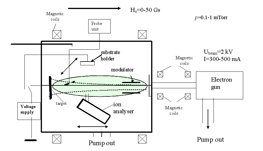
isolated structures - the modulation of the plasma potential due to collector supply
with pulse voltage. In a DLC film deposition mode (see lower) this voltage
feeds a special electrode at region of the discharge. A specific
modulator has been designed and manufactured for this aim. The modulator
provides the generation of pulsed voltage with amplitude of 50-150 V at load
≤1 A in the range of operating frequencies 100-400 kHz. The
modulator can operate at off-duty factor ≥ 2.
Accomplished
technologies.
1. Low energy etching of
heterostructures
The test of etching technology with ion
flows from BPD has been conducted for semiconductor heterostructures Al-GaAs/InGaAs/GaAs
(P-HEMT), grown on GaAs substrates. These structures are promising in creating
the microwave field transistors of millimeter band. The effect of such treatment
on the concentration and mobility of the electrons was studied. These
parameters are sensitive to defects caused by the etching process. We have shown
the existence of the etching effect at a rate acceptable for industrial
applications, without the heterostructure parameters’ degrading indicating a low-density
radiation-induced disorders and the possibility of using BPD in manufacturing
technology of HEMT heterostructure microwave devices [3,
6].
Russian patent on “Method of plasma
chemical etching of semiconductor and dielectric materials” ((ą2316845,
priority date 06.06.2006 g., entr. ą 021244, reg. 10.02.2008). Applicant – Kotel'nikov Institute of Radio Engineering and Electronics of RAS, the authors
of the invention – N.V. Isaev, Yu.V. Fedorov, E.G. Shustin.
2. Production of graphene (the work
is done in conjunction with the laboratory 184 –
http: / / www.cplire.ru /nano /index.html)
A monolayer of
graphite - graphene, isolated recently in a free state under normal conditions, demonstrates unique physical properties of
two-dimensional system containing massless carriers - Dirac fermions, as well
as high promising application capabilities in creating new generation of field effect
transistors, transparent conductive electrodes, etc. The first samples of
graphene, obtained by mechanical cleavage of graphite, have a lateral size of
the order of several microns and can be used only for laboratory research. Practical
realization of nanostructures based on graphene in electronics and optoelectronics
has raised the question of obtaining high quality, large area graphene samples.
Significant
progress has recently been achieved by the method of chemical deposition of
graphene from the gaseous phase (CVD method) on the Ni-substrate, followed by transferring
it to arbitrary substrate. Although, thus obtained solid graphene films have a
large area, they have microscopically large variations in thickness from ten to
one graphite layers. Relevant domains of one-and two-layer graphene have a
lateral size of about 5 microns.
An alternative method for obtaining
graphene films is proposed [7] by means of etching of thin defect-free single graphite
crystals in the reactor based on beam-plasma discharge. The perspective of this
method is determined by the high structural perfection of initial single
graphite crystals to be etched and their large area.
The graphite crystals with a thickness of
30-100 nm and lateral size of several hundred microns were obtained by cleavage
of single crystals of natural graphite with adhesive tape. Tape adhesive agent was
then dissolved in acetone, and thin crystal became free floating in the
solvent. At the next stage the crystal was transferred to the firm substrate.
At the last stage the crystal was thinned
by means of plasma etching which was carried out in the beam-plasma reactor. The
argon-ion energy was 80 eV at the initial stage of etching and decreased to 60
eV at the final stage, thus ensuring flawless soft mode of etching at a rate
about 10 nm/hour. The thickness of films was monitored by their resistance in
situ in the plasma reactor chamber. Etching was stopped at the sheet
resistance of the film ~ 1 kOhm, corresponding to conductivity of 1-2-layered
graphene. Scanning the local Raman spectra with a step of 0.2 mm showed high
structural perfection of thus obtained 1-2-layered graphene films (fig. 2) and
its uniformity in thickness over a large area in excess of 100*100 mm2.
The method of this production of one- or two-atomic
layers can be extended to other layered materials. To make the process of
thinning not too long, the thickness of the original crystal should not exceed
50-100 nm. Single crystal to be thinned can be put be put onto any substrate. Therefore,
the proposed method can be implemented in any substrates, including flexible
ones.
Application for Russian patent “Method
of obtaining atomic-thin single-crystal films”, ą 2009142861 dated 23.11.2009.
3. Deposition of diamond-like
carbon films (work done in conjunction with the laboratory 197 -
http://fire.relarn.ru/index.htm?main=197/index.htm)
In the worldwide practice low-pressure plasma
reactors based on RF and microwave discharges are widely used for the
deposition of diamond-like carbon (DLC) films. The film characteristics are
critically dependent on the composition of the plasma creating gas, the discharge
regime parameters and the substrate surface quality. In [8] a special
modification of the BPD, which we called “reflective BPD”, is proposed to be used
for the deposition of DLC films. At this modification graphite disc with a
diameter of 10 cm is used as a collector and a target, which is fed with cathode
potential. Thus, the target is bombarded by the flow of ions of energy up to 2 keV
from the discharge. In this mode, the electron density of plasma increases (1,5
- 3 times in relation to the usual scheme) and plasma potential relative to the
chamber walls decreases. Oscillating voltage is applied to a special modulating
electrode (see. figure 1) to control the ion flux density and energy. This modification
of plasma-chemical reactor for deposition of DLC films differs from the known
methods by simple control of the energy characteristics of the ion flux affecting
the film during the deposition. Samples of DLC films on metallic substrates have
been produced. The effect of adsorbed water vapor and alcohol on the electrical
properties of films has been revealed by means of the method of
charge-relaxation spectroscopy, that indicates the possibility of using the
film as an active adsorbent material for chemical sensors. Studies of the
influence of ion energy and other reactor parameters on the electrical
properties of the deposited films continue.
MAIN REFERENCES
-
N. V.
Isaev, A. I. Chmil’, and E. G. Shustin. Ion Flows from a Beam–Plasma Discharge //Plasma Phys. Rep. 2004; 30: p.263
-
N. V.
Isaev, A. A. Rukhadze, and E. G. Shustin. Mechanism
for Ion Acceleration along the Normal to the Axis of a Beam–Plasma Discharge in a Weak Magnetic
Field Plasma //Phys. Rep. 2005,31, p. 953
- N.V. Isaev, V.P. Tarakanov, E.G. Shustin Ion flows from area of beam plasma discharge at low magnetic
field – physics and application //Problems of atomic science and technology,
Serial 5. ”Plasma electronics a. New methods of acceleration”, NAN of
Ukraina, , 2006 No5, p. 100
-
N. V. Isaev
and E. G. Shustin.
Acceleration of Ions in a Beam–Plasma Discharge in a Low Magnetic
Field:Interrelation between the Electron and Ion Energy Distributions //Plasma Phys. Rep. 2007; 33 p. 38
-
V. P.
Tarakanov and E. G. Shustin. Dynamics of Beam Instability in a Finite Plasma Volume: Numerical
Experiment. //Ibid.,p.130
- E.G. Shustin, N.V. Isaev, M.P.
Temiryazeva, Yu.V. Fedorov. Beam plasma
discharge at low magnetic field as plasma source for plasma processing
reactor. //Vacuum 2009, v.83 No11, pp.1350
- Yu.I. Latyshev, Ĺ.G. Shustin, Ŕ.Yu. Latyshev,
N.V. Isaev, Ŕ.Ŕ. Schekin, V.Ŕ. Bykov. Novel
method of production of graphene films of large area inplasma discharge. //Report
on 2 Intern. Nanoforum, Moscow 2009,
http://rusnanotech09.rusnanoforum.ru/Public/LargeDocs/theses/eng/poster/09/10_Latyshev.pdf
- N.V. Isaev, I.L. Klykov, V.V. Peskov,
E.G. Shustin. Beam plasma processing reactor
at diamond-like film deposition mode// XXXVII international conference on
plasma physics and CF, February 8 – 12, 2010, Zvenigorod.
http://www.fpl.gpi.ru/Zvenigorod/XXXVII/Pt/en/OZ-Shustin_e.doc
Beam plasma reactor schematic